- 您现在的位置:买卖IC网 > Sheet目录868 > LTM4603HVEV#PBF (Linear Technology)IC DC/DC UMODULE 6A 118-LGA
�� �
�
�LTM4603HV�
�APPLICATIO� S� I� FOR� ATIO�
�Safety� Considerations�
�The� LTM4603HV� modules� do� not� provide� isolation� from�
�V� IN� to� V� OUT� .� There� is� no� internal� fuse.� If� required,� a� slow�
�blow� fuse� with� a� rating� twice� the� maximum� input� current�
�needs� to� be� provided� to� protect� each� unit� from� catastrophic�
�failure.�
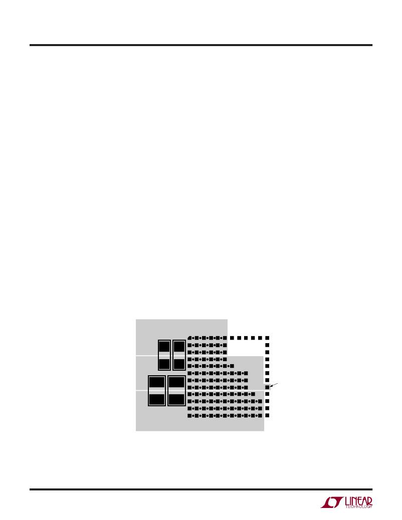
�Layout� Checklist/Example�
�The� high� integration� of� LTM4603HV� makes� the� PCB� board�
�layout� very� simple� and� easy.� However,� to� optimize� its� electri-�
�cal� and� thermal� performance,� some� layout� considerations�
�are� still� necessary.�
�?� Use� large� PCB� copper� areas� for� high� current� path,� in-�
�cluding� V� IN� ,� PGND� and� V� OUT� .� It� helps� to� minimize� the�
�PCB� conduction� loss� and� thermal� stress.�
�?� Place� high� frequency� ceramic� input� and� output� capaci-�
�tors� next� to� the� V� IN� ,� PGND� and� V� OUT� pins� to� minimize�
�high� frequency� noise.�
�?� Place� a� dedicated� power� ground� layer� underneath� the�
�unit.�
�?� To� minimize� the� via� conduction� loss� and� reduce� module�
�thermal� stress,� use� multiple� vias� for� interconnection�
�between� top� layer� and� other� power� layers.�
�V� IN�
�?� Do� not� put� vias� directly� on� pads.�
�?� If� vias� are� placed� onto� the� pads,� the� the� vias� must� be�
�capped.�
�?� Interstitial� via� placement� can� also� be� used� if� necessary.�
�?� Use� a� separated� SGND� ground� copper� area� for� com-�
�ponents� connected� to� signal� pins.� Connect� the� SGND�
�to� PGND� underneath� the� unit.�
�Figure� 17� gives� a� good� example� of� the� recommended�
�layout.�
�Frequency� Adjustment�
�The� LTM4603HV� is� designed� to� typically� operate� at� 1MHz�
�across� most� input� conditions.� The� f� SET� pin� is� typically� left�
�open� or� decoupled� with� an� optional� 1000pF� capacitor.� The�
�switching� frequency� has� been� optimized� for� maintaining�
�constant� output� ripple� noise� over� most� operating� ranges.�
�The� 1MHz� switching� frequency� and� the� 400ns� minimum�
�off� time� can� limit� operation� at� higher� duty� cycles� like� 5V� to�
�3.3V,� and� produce� excessive� inductor� ripple� currents� for�
�lower� duty� cycle� applications� like� 28V� to� 5V.� The� 5V� and�
�3.3V� drop� out� curves� are� modi?ed� by� adding� an� external�
�resistor� on� the� f� SET� pin� to� allow� for� wider� input� voltage�
�operations.�
�C� IN�
�C� IN�
�GND�
�SIGNAL�
�GND�
�C� OUT�
�C� OUT�
�V� OUT�
�4603HV� F17�
�Figure� 17.� Recommended� Layout�
�4603hvf�
�18�
�发布紧急采购,3分钟左右您将得到回复。
相关PDF资料
LTM4603IV#PBF
IC DC/DC UMODULE 6A 118-LGA
LTM4604AIV#PBF
IC UMODULE DC/DC LV 4A 66-LGA
LTM4604IV#PBF
IC DC/DC UMODULE 4A 66-LGA
LTM4605EV#PBF
IC DC/DC UMODULE 5A 141-LGA
LTM4606MPV#PBF
IC DC/DC UMODULE 6A 133-LGA
LTM4607IV#PBF
IC BUCK/BOOST SYNC ADJ 5A 141LGA
LTM4608AEV#PBF
IC BUCK SYNC ADJ 8A 68LGA
LTM4608IV#PBF
IC DC/DC UMODULE 8A 68-LGA
相关代理商/技术参数
LTM4603HVEV#PBF
制造商:Linear Technology 功能描述:DC/DC Converter IC
LTM4603HVEV-1#PBF
制造商:Linear Technology 功能描述:6A 28V DCDC UMODULE: NO REMOTE
LTM4603HVEVPBF
制造商:Linear Technology 功能描述:6A 28V input DCDC uModule LTM4603HV
LTM4603HVEV-PBF
制造商:LINER 制造商全称:Linear Technology 功能描述:6A, 28VIN DC/DC μModule with PLL, Output Tracking and Margining
LTM4603HVIV#PBF
功能描述:IC DC/DC UMODULE 6A 118-LGA RoHS:是 类别:电源 - 板载 >> DC DC Converters 系列:µModule® 设计资源:VI-200, VI-J00 Design Guide, Appl Manual 标准包装:1 系列:* 类型:隔离 输出数:1 电压 - 输入(最小):36V 电压 - 输入(最大):76V Voltage - Output 1:5.5V Voltage - Output 2:- Voltage - Output 3:- 电流 - 输出(最大):* 电源(瓦) - 制造商系列:200W 电压 - 隔离:* 特点:* 安装类型:通孔 封装/外壳:9-FinMod 尺寸/尺寸:4.60" L x 1.86" W x 1.05" H(116.8mm x 47.2mm x 26.7mm) 包装:散装 工作温度:-10°C ~ 85°C 效率:* 电源(瓦特)- 最大:*
LTM4603HVIV#PBF
制造商:Linear Technology 功能描述:DC/DC Converter IC
LTM4603HVIV-PBF
制造商:LINER 制造商全称:Linear Technology 功能描述:6A, 28VIN DC/DC μModule with PLL, Output Tracking and Margining
LTM4603HVV
制造商:LINER 制造商全称:Linear Technology 功能描述:6A, 28VIN DC/DC μModule with PLL, Output Tracking and Margining